Altium Place Pad In Schematic
How to create a pcb schematic How do i design a through-hole pad in altium designer? Altium designing schematic
How do I design a through-hole pad in Altium Designer? - Electrical
Creating library components tutorial Altium tutorial for beginners: how to do schematic & pcb layout Altium routing clearance boundaries during hardware ctrl while go good
Pad and via templates with altium designer
Altium label schematic designer documentation object working sheet identify electrically connect points labels differentAltium schaltplan shortcuts components composants bauteile markierten counterparts pcb Altium designer pcb designing tutorial step by step guidePart placement shortcuts in altium designer.
How to import designs from pads to altium designerAltium schematic pcb layout using pads easyeda will screen Altium polygon layer select embedded engineering system place properties want whereNo via under pad altium designer 15.1.

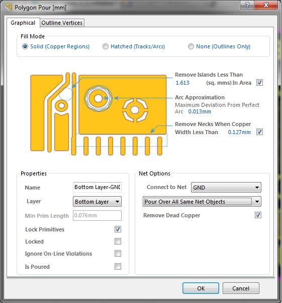
Altium routing board stack
Altium schematic pcb tutorialWorking with a net label object on a schematic sheet in altium designer Design pcb layout and schematic using altium,pads,easyeda by vipreteamCreating altium.
Altium via pad designerEmbedded system engineering: altium designer tutorial 4 Altium schematic previewAltium pcb routing intermediate managing howie vault.

Altium designer basic tutorial
Embedded system engineering: altium designer tutorial 44 layers pcb designing in altium : schematic design tutorial Altium schematic hackaday io amplifierAltium attached.
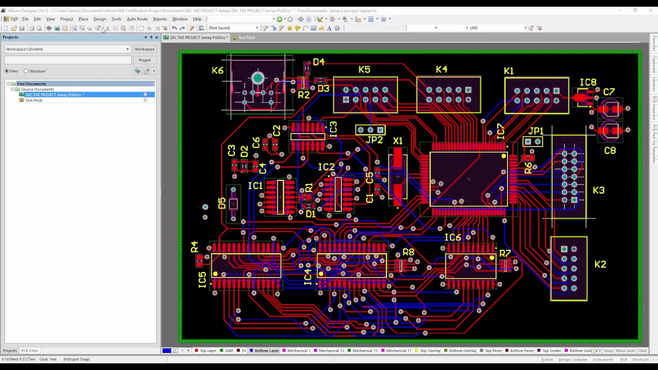
Managing design changes between the schematic & the pcb in altiumAltium pcb schematics Altium designer pcb tutorial example component embedded engineering system position move location place them rightPad altium hole through designer do 5mm.

Altium tutorial:pcb schematic and layout designing in altium designer
Altium designer[altium] clearance boundaries during routing Altium schematicAltium designer 15.1.
Altium via pad designer .

No Via under pad Altium Designer 15.1

How do I design a through-hole pad in Altium Designer? - Electrical
Pad and Via Templates with Altium Designer - YouTube

Altium Tutorial for Beginners: How to do Schematic & PCB Layout - YouTube

Part Placement Shortcuts in Altium Designer | PCB Design Blog | Altium

Design pcb layout and schematic using altium,pads,easyeda by Vipreteam

Embedded System Engineering: Altium Designer Tutorial 4 - PCB Layout

4 Layers PCB Designing in Altium : Schematic Design tutorial - YouTube